LED is a light-emitting device that directly converts electrical energy into visible light and radiant energy. It has the advantages of low power consumption, high luminous efficiency, and small size. It has gradually become a new type of high-efficiency and energy-saving product, and is widely used in display , lighting, backlight and many other fields. In recent years, with the continuous advancement of LED technology, its luminous efficiency has also been significantly improved. The existing blue LED system efficiency can reach 60%, while the luminous efficacy of white LED has exceeded 150lm/W. These characteristics make LEDs subject to More and more attention.
Although the theoretical life of LED can reach more than 50kh, due to the limitations of various factors, LED usually cannot reach such a high theoretical life in practical application, and premature failure occurs, which greatly hinders the development of LED, a new type of energy-saving product. . In order to solve this difficult problem, many scholars have carried out relevant research and drawn some meaningful conclusions.
#1 Case Background:
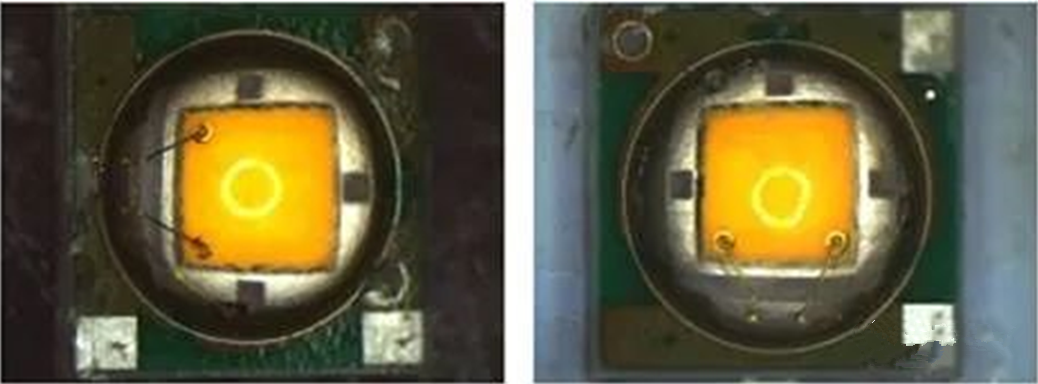
The LED does not light up when it is powered on, but it can be illuminated normally when lightly pressed by hand.
#2 Analysis Process
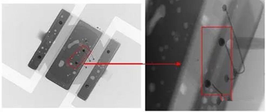
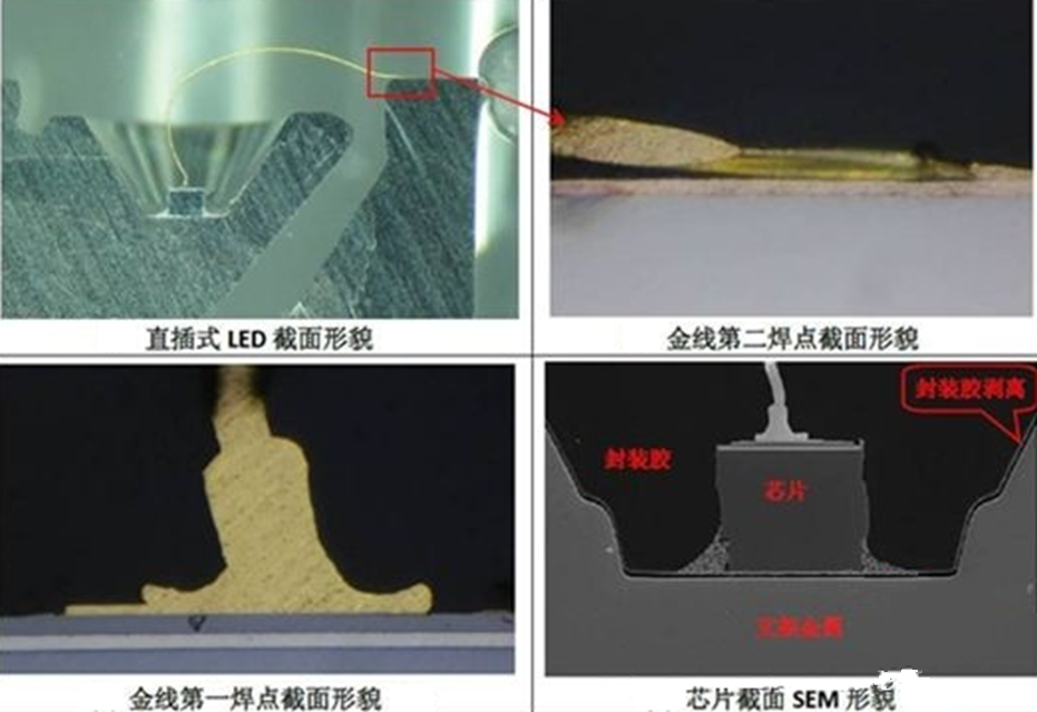
X-ray perspective can clearly find that the two binding wires on the NG sample connected to the large chip inside the LED have obvious breaks at the ends of the binding points, and the end connected to the negative electrode inside is well bound. Normal samples showed no abnormalities.
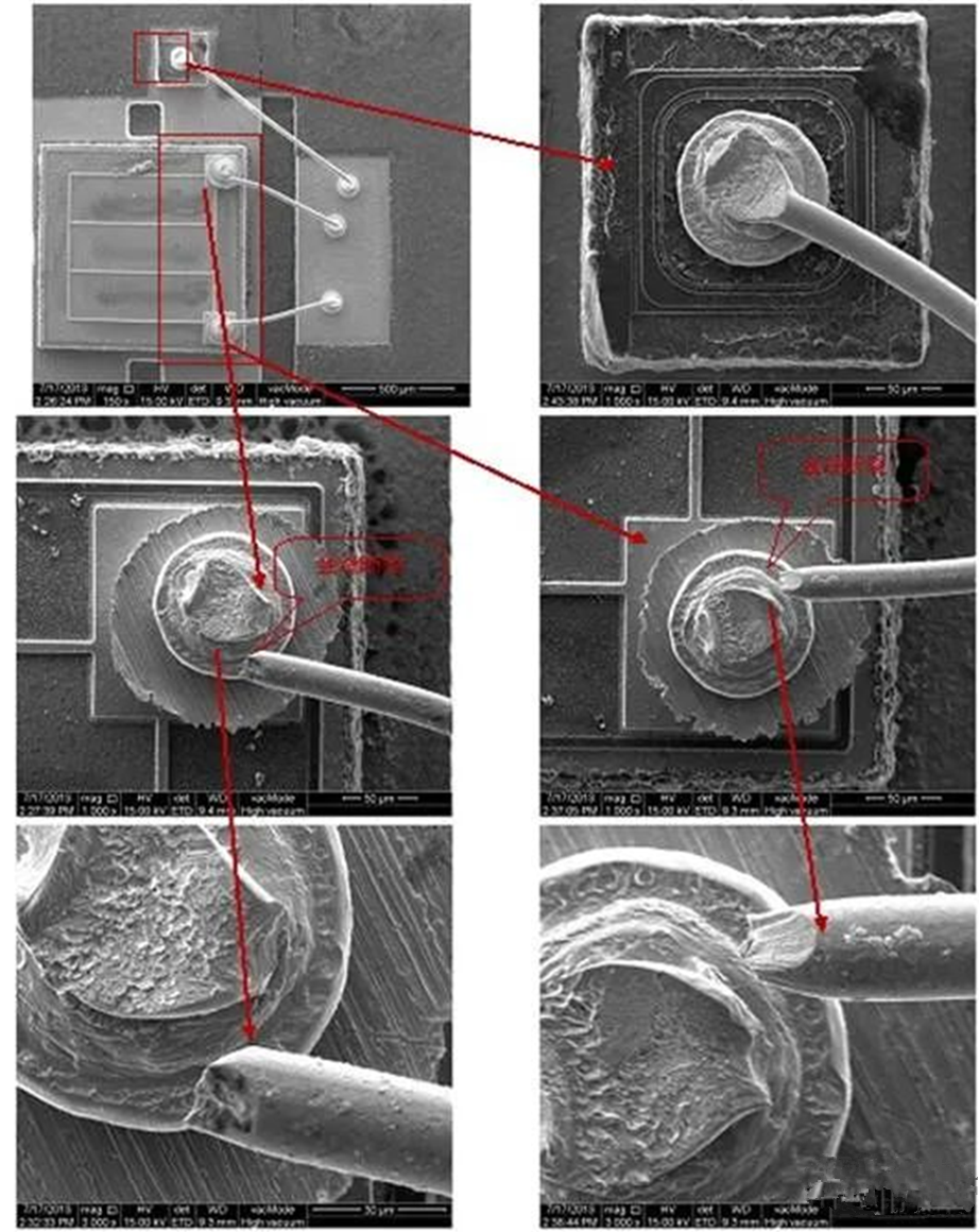
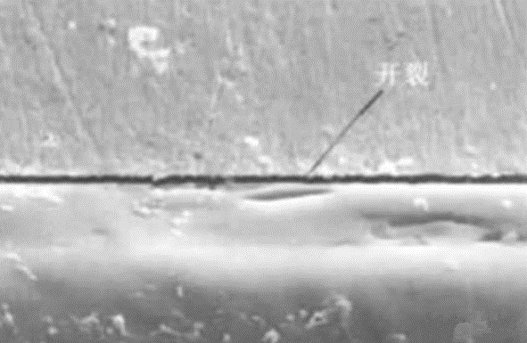
Using chemical methods to corrode the encapsulation colloid on the surface of the LED lamp, and observing the internal structure through an electron microscope, it can be clearly found that significant mechanical stress cracks have occurred at the ends of the two gold wires connected to the positive electrode in the chip. Necking and metal mechanical cusps appear on the surface. The broken parts are all located at the binding neck, and the binding effect is better at the binding point. Sectional observation did not reveal packaging defects such as obvious cracks and pores in the LED hemispherical sealing body.
According to the internal structure of the LED after opening, the sample is different from the ordinary LED package. The positive bonding point of the chip is the second bonding point with fins (usually the second bonding point is weaker when the chip is packaged, and it is prone to cracks and other abnormalities. case), and the binding point at the negative pole of the frame is opposite the first binding point in the sphere. It is precisely the second binding point with the tail that occurs the mechanical fracture. This position is higher than the first binding point of the negative electrode in the three-dimensional space and is greatly affected by the external mechanical stress.
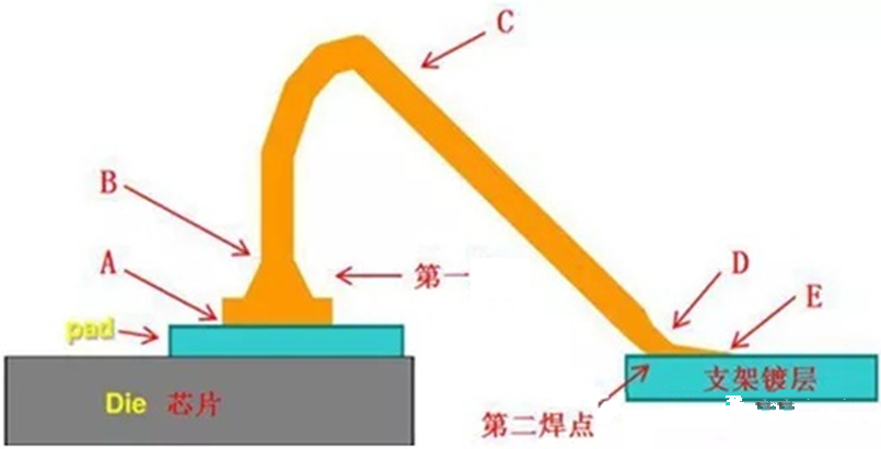
- Point A, the junction of the chip electrode and the gold ball;
- Point B, the junction of the gold ball and the gold wire is the neck of the ball;
- Point C, the range where the arc of the welding wire is located;
- Point D, the junction of the second solder point of the bracket and the gold wire;
- Point E is the junction of the second welding point of the bracket and the coating of the bracket.
#3 Failure Mode
1. Chip failure
Wafer failure refers to the failure of the wafer itself or the failure of the wafer caused by other reasons. There are often many reasons for this failure. Chip cracks are caused by improper bonding process conditions, resulting in greater stress, and the thermomechanical stress generated by heat accumulation is also strengthened, resulting in micro-cracks in the chip. The injected current will further aggravate the microcracks and make them continue to expand until they fail completely. The second is that if the active area of the chip is originally damaged, it will gradually deteriorate to failure when power is applied, and also cause serious light decay to no light when the lamp is running. In addition, if the chip bonding process is not good, the chip bonding layer will be completely separated from the bonding surface during use, causing the sample to open and fail, which will also cause “dead lights” when the LED is used. The reason for poor chip bonding process may be that the silver paste (insulating glue) used has expired or the exposure time is too long, the amount of silver paste (insulating glue) is too small, the curing time is too long, and the crystal bonding surface is contaminated.
2. Package failure
Package failure refers to the failure of the device due to improper package design or production process. The epoxy resin material used for packaging will deteriorate during use, resulting in a reduction in the life of the LED. This degradation problem includes light transmittance, refractive index, expansion coefficient, hardness, water permeability, air permeability, filler performance, etc., among which light transmittance is the most important. Some studies have shown that the shorter the wavelength of light, the more serious the deterioration of light transmittance, but the impact on wavelengths above green light (ie greater than 560nm) is not significant. In 2003, Lumileds published the life experiment curves of power LED white light devices and φ5 white light devices. After 19kh, the luminous flux of power devices encapsulated with silicone resin can still maintain 80% of the original. The comparison curve of epoxy resin packaging shows that the luminous flux maintenance rate is only 50% after 6kh. It is proved that when the luminous efficiency of the chip remains unchanged, the epoxy resin near the chip changes significantly to yellow, and then turns to brown. This significant degradation process is mainly caused by the deterioration of the light transmittance of epoxy resin caused by light and temperature rise. At the same time, when the blue light stimulates the yellow phosphor to emit white light, the browning of the LED package lens will affect the reflectivity, and make the blue light insufficient to stimulate the yellow phosphor to change the light effect and spectral distribution.
For packaging, another important factor that affects the life of LEDs is corrosion. In the use of LEDs, the main cause of corrosion is that water vapor penetrates into the packaging material, leading to deterioration of leads and corrosion of PCB copper wires; sometimes, movable conductive ions introduced with water vapor will reside on the surface of the chip, resulting in leakage. In addition, devices with poor packaging quality will have a large number of residual bubbles inside the package, and these residual bubbles will also cause corrosion of the device.
3. Thermal overstress failure
Temperature has always been an important factor affecting the optical properties of LEDs. When studying LED failure modes, scholars at home and abroad consider the working environment temperature as the accelerated stress to conduct LED accelerated life experiments. This is because on the premise that the thermal resistance of the LED system remains unchanged, if the temperature of the soldering point of the package pin increases, the junction temperature will also increase accordingly, resulting in premature failure of the LED. The model structure diagram of the high-power LED and the relationship between the radiation power and the acceleration time at the working ambient temperature of (a) 120°C, (b) 100°C and (c) 80°C respectively are as follows.
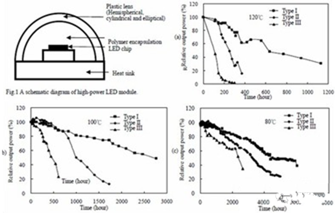
In the accelerated life experiment of LED samples provided by different manufacturers, the LED samples were placed at 80, 100, and 120°C respectively, driven by a voltage of 3.2V, and it was stipulated that when the optical power of the sample dropped to the initial value 50% will be deemed invalid. The test results in the figure above show that the life of high-power LEDs decreases with the acceleration of life test temperature and acceleration time. In the accelerated life test, the increase of the LED junction temperature will cause the epoxy resin material to change, which will increase the thermal resistance of the system, degrade the heated surface of the chip and package, and eventually cause the package to fail.
4.Electrical Overstress Failure
If the LED is affected by factors such as overcurrent (EOS) or electrostatic shock (ESD), it may cause the chip to open and form an electrical overstress fault. For example, GaN is a wide bandgap material with high resistivity. If this kind of chip is used, the induced charge caused by static electricity is not easy to disappear during the manufacturing process. When it accumulates to a certain extent, a high electrostatic voltage can be generated. Once the voltage exceeds the material’s capacity, breakdown will occur And discharge phenomenon, make the device malfunction.
5.Bond Failure
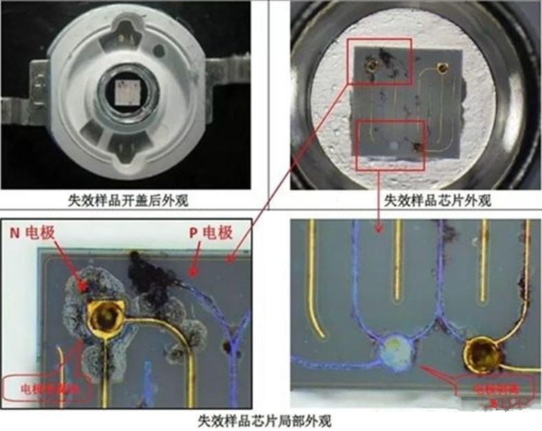
Improper bonding conditions in the LED manufacturing process. If the bonding force is too large, the wafer will be crushed. Otherwise, the bonding strength of the device will be insufficient, making the device easy to loosen, or a good bonding interface will not be formed at all. For some LED lamp beads using vertical chips, the peeling off of the bottom of the die-bonding layer from the coating of the bracket is a common cause of failure. The fault sample in the picture below is the dead light phenomenon of the in-line LED lamp bead during use, and the defect rate is 1.5%. Cross-sectional inspection of the failed sample showed that the gold wire solder joints were all intact. However, it was found that the die-bonding layer was completely peeled off from the stent plating, and at the same time, the encapsulant was peeled off from the stent cup wall.
From the above observations, it can be judged that the cause of the failure of the lamp bead is the peeling phenomenon between the packaging glue and the bracket interface. The degree of peeling and the area expand with the intensification of the use process, which further causes the peeling of the die-bonding glue and the bracket, and finally leads to the failure of the sample. A failure occurred. It may also be that the poor adhesion of the encapsulation glue causes delamination between the encapsulation glue and the bracket interface.
6.Mechanical Stress Failure
During the flow, test or transportation of LED in SMT process, external fixtures, molds or other hard materials hit the LED lamp package, causing its internal structure to shift instantly and break the internal binding wire. This type of failure is more likely to be found in softer packages.
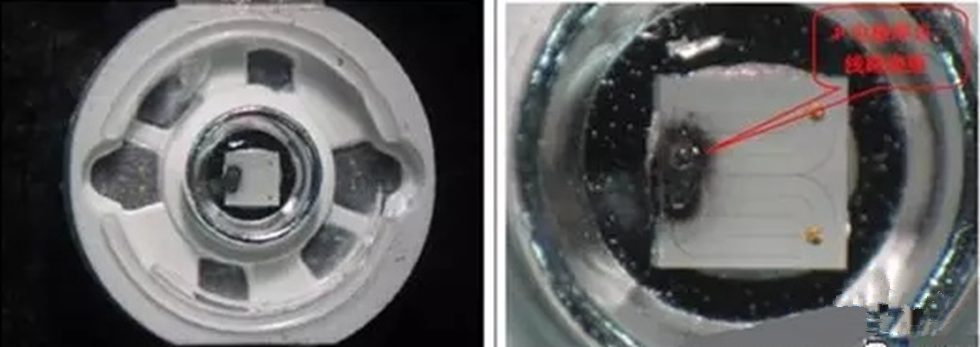
LED chips are composed of semiconductor materials such as InGaN, AlInGaP and ZnSe, which are often thinner and more brittle than Si chips. If the packaging design is improper, there will be residual stress inside, and the existence of these stresses may lead to reliability problems such as device chip cracking and functional degradation. The case analyzed in the figure below is also a large number of failures after the LED samples were placed on the board. The failure analysis of the LED samples found that all the LED chips had cracks, and the cracks were located in the same position, all located in the right area of the chip, that is, near the right edge of the anode lead-out piece. The crack runs through the PN junction, and the PN withstand voltage at the crack is severely reduced. Moreover, in a humid environment, the leakage of the crack at the PN junction increases. The generation of cracks is related to mechanical stress.
According to the failure information of the sample, combined with the substrate structure of the chip and the electrical connection method of the chip (bumps are welded by flip-chip instead of ordinary gold wire), the reason for the cracking of the LED chip is analyzed that the mechanical stress is between the two electrodes of the LED chip. A relative shear force is formed between them, and corresponding solutions are proposed. The force is directly applied to the LED chip through the bumps, so that the thin and brittle LED chip produces force cracks. There is a certain relationship between mechanical stress and thermal stress.
#4 Improvement Measures:
Through the analysis of the main failure modes of LEDs introduced above, we can learn the technical methods to improve the actual service life of LEDs.
1. Heat Dissipation Technology
Heat dissipation technology has always been an important part of LED applications. If the LED device cannot dissipate heat in time, the junction temperature of the chip will rise severely, and then the luminous efficiency will be greatly reduced, and the reliability (such as lifespan, color shift, etc.) will also deteriorate. At the same time, high temperature and high heat will cause mechanical stress in the LED packaging structure and may further cause a series of reliability problems. Therefore, in the production process, a base with good thermal conductivity can be selected and the heat dissipation area of the LED should be as large as possible to improve the heat dissipation performance of the device.
2. Anti-static technology
One of the biggest problems in the use of GaN-based LEDs is the electrostatic effect. If this problem is not dealt with properly, it will seriously affect the life of the device. Therefore, when designing LEDs, it is necessary to fully consider the anti-static design to avoid failures such as breakdown of devices due to high electrostatic voltage.
3. Packaging technology
The light transmittance of the epoxy resin material for packaging deteriorates due to light and temperature rise, and the original transparent epoxy resin material browns during use, which affects the original spectral power distribution of the device. Therefore, when the LED packaging is completed, the curing temperature should be strictly controlled to avoid premature aging of the epoxy resin after the packaging is completed. On the other hand, in order to avoid corrosion of the device, when choosing a packaging material with good transparency, attention should be paid to expel the air bubbles in the material as much as possible during injection molding, in order to reduce the residual moisture and reduce the possibility of corrosion of the device.
4. Optimizing the manufacturing process
LEDs need to have proper bonding conditions during the manufacturing process. If the bonding is too large, the chip will be crushed, otherwise it will lead to insufficient bonding strength of the device, making the device easy to loosen. Therefore, under the premise of ensuring the bonding strength of the device, it is necessary to reduce the damage to the chip during the bonding process as much as possible, so as to realize the optimization of the bonding process. In the process of bonding chips, it is necessary to control the temperature within an appropriate range so that the solder meets the technical requirements of denseness, no voids, and low residual stress.
5. Reasonable screening
Before the LED leaves the factory, a screening process can be added, that is, through a reasonable aging screening test on some samples to exclude some equipment with the possibility of premature failure, so as to reduce the premature failure of the LED in actual application.
#5 Case Conclusion
The main reason why the LED of the failed sample did not light up when it was powered on, but lightly pressed by hand (open circuit) was mainly due to the mechanical stress rupture of the second bonding point of the internal chip of the NG sample under the action of external mechanical stress.